In 1985, Intel introduced the groundbreaking 386 processor, the first 32-bit processor in the x86 architecture. To improve performance, the 386 has a 16-byte instruction prefetch queue. The purpose of the prefetch queue is to fetch instructions from memory before they are needed, so the processor usually doesn't need to wait on memory while executing instructions. Instruction prefetching takes advantage of times when the processor is "thinking" and the memory bus would otherwise be unused.
In this article, I look at the 386's prefetch queue circuitry in detail. One interesting circuit is the incrementer, which adds 1 to a pointer to step through memory. This sounds easy enough, but the incrementer uses complicated circuitry for high performance. The prefetch queue uses a large network to shift bytes around so they are properly aligned. It also has a compact circuit to extend signed 8-bit and 16-bit numbers to 32 bits. There aren't any major discoveries in this post, but if you're interested in low-level circuits and dynamic logic, keep reading.
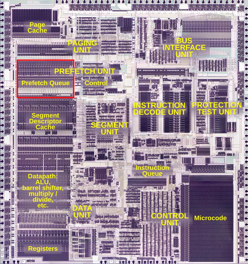
The photo below shows the 386's shiny fingernail-sized silicon die under a microscope. Although it may look like an aerial view of a strangely-zoned city, the die photo reveals the functional blocks of the chip. The Prefetch Unit in the upper left is the relevant block. In this post, I'll discuss the prefetch queue circuitry (highlighted in red), skipping over the prefetch control circuitry to the right. The Prefetch Unit receives data from the Bus Interface Unit (upper right) that communicates with memory. The Instruction Decode Unit receives prefetched instructions from the Prefetch Unit, byte by byte, and decodes the opcodes for execution.
 for a larger version.")
This die photo of the 386 shows the location of the registers. Click this image (or any other) for a larger version.
The left quarter of the chip consists of stripes of circuitry that appears much more orderly than the rest of the chip. This grid-like appearance arises because each functional block is constructed (for the most part) by repeating the same circuit 32 times, once for each bit, side by side. Vertical data lines run up and down, in groups of 32 bits, connecting the functional blocks. To make this work, each circuit must fit into the same width on the die; this layout constraint forces the circuit designers to develop a circuit that uses this width efficiently without exceeding the allowed width. The circuitry for the prefetch queue uses the same approach: each circuit is 66 µm wide1 and repeated 32 times. As will be seen, fitting the prefetch circuitry into this fixed width requires some layout tricks.
What the prefetcher does
The purpose of the prefetch unit is to speed up performance by reading instructions from memory before they are needed, so the processor won't need to wait to get instructions from memory. Prefetching takes advantage of times when the memory bus is otherwise idle, minimizing conflict with other instructions that are reading or writing data. In the 386, prefetched instructions are stored in a 16-byte queue, consisting of four 32-bit blocks.2
The diagram below zooms in on the prefetcher and shows its main components. You can see how the same circuit (in most cases) is repeated 32 times, forming vertical bands. At the top are 32 bus lines from the Bus Interface Unit. These lines provide the connection between the datapath and external memory, via the Bus Interface Unit. These lines form a triangular pattern as the 32 horizontal lines on the right branch off and form 32 vertical lines, one for each bit. Next are the fetch pointer and the limit register, with a circuit to check if the fetch pointer has reached the limit. Note that the two low-order bits (on the right) of the incrementer and limit check circuit are missing. At the bottom of the incrementer, you can see that some bit positions have a blob of circuitry missing from others, breaking the pattern of repeated blocks. The 16-byte prefetch queue is below the incrementer. Although this memory is the heart of the prefetcher, its circuitry takes up a relatively small area.

A close-up of the prefetcher with the main blocks labeled. At the right, the prefetcher receives control signals.
The bottom part of the prefetcher shifts data to align it as needed. A 32-bit value can be split across two 32-bit rows of the prefetch buffer. To handle this, the prefetcher includes a data shift network to shift and align its data. This network occupies a lot of space, but there is no active circuitry here: just a grid of horizontal and vertical wires.
Finally, the sign extend circuitry converts a signed 8-bit or 16-bit value into a signed 16-bit or 32-bit value as needed. You can see that the sign extend circuitry is highly irregular, especially in the middle. A latch stores the output of the prefetch queue for use by the rest of the datapath.
Limit check
If you've written x86 programs, you probably know about the processor's Instruction Pointer (EIP) that holds the address of the next instruction to execute. As a program executes, the Instruction Pointer moves from instruction to instruction. However, it turns out that the Instruction Pointer doesn't actually exist! Instead, the 386 has an "Advance Instruction Fetch Pointer", which holds the address of the next instruction to fetch into the prefetch queue. But sometimes the processor needs to know the Instruction Pointer value, for instance, to determine the return address when calling a subroutine or to compute the destination address of a relative jump. So what happens? The processor gets the Advance Instruction Fetch Pointer address from the prefetch queue circuitry and subtracts the current length of the prefetch queue. The result is the address of the next instruction to execute, the desired Instruction Pointer value.
The Advance Instruction Fetch Pointer—the address of the next instruction to prefetch—is stored in a register at the top of the prefetch queue circuitry. As instructions are prefetched, this pointer is incremented by the prefetch circuitry. (Since instructions are fetched 32 bits at a time, this pointer is incremented in steps of four and the bottom two bits are always 0.)
But what keeps the prefetcher from prefetching too far and going outside the valid memory range? The x86 architecture infamously uses segments to define valid regions of memory. A segment has a start and end address (known as the base and limit) and memory is protected by blocking accesses outside the segment. The 386 has six active segments; the relevant one is the Code Segment that holds program instructions. Thus, the limit address of the Code Segment controls when the prefetcher must stop prefetching.3 The prefetch queue contains a circuit to stop prefetching when the fetch pointer reaches the limit of the Code Segment. In this section, I'll describe that circuit.
Comparing two values may seem trivial, but the 386 uses a few tricks to make this fast. The basic idea is to use 30 XOR gates to compare the bits of the two registers. (Why 30 bits and not 32? Since 32 bits are fetched at a time, the bottom bits of the address are 00 and can be ignored.) If the two registers match, all the XOR values will be 0, but if they don't match, an XOR value will be 1. Conceptually, connecting the XORs to a 32-input OR gate will yield the desired result: 0 if all bits match and 1 if there is a mismatch. Unfortunately, building a 32-input OR gate using standard CMOS logic is impractical for electrical reasons, as well as inconveniently large to fit into the circuit. Instead, the 386 uses dynamic logic to implement a spread-out NOR gate with one transistor in each column of the prefetcher.
The schematic below shows the implementation of one bit of the equality comparison. The mechanism is that if the two registers differ, the transistor on the right is turned on, pulling the equality bus low. This circuit is replicated 30 times, comparing all the bits: if there is any mismatch, the equality bus will be pulled low, but if all bits match, the bus remains high. The three gates on the left implement XNOR; this circuit may seem overly complicated, but it is a standard way of implementing XNOR. The NOR gate at the right blocks the comparison except during clock phase 2. (The importance of this will be explained below.)

This circuit is repeated 30 times to compare the registers.
The equality bus travels horizontally through the prefetcher, pulled low if any bits don't match. But what pulls the bus high? That's the job of the dynamic circuit below. Unlike regular static gates, dynamic logic is controlled by the processor's clock signals and depends on capacitance in the circuit to hold data. The 386 is controlled by a two-phase clock signal.4 In the first clock phase, the precharge transistor below turns on, pulling the equality bus high. In the second clock phase, the XOR circuits above are enabled, pulling the equality bus low if the two registers don't match. Meanwhile, the CMOS switch turns on in clock phase 2, passing the equality bus's value to the latch. The "keeper" circuit keeps the equality bus held high unless it is explicitly pulled low, to avoid the risk of the voltage on the equality bus slowly dissipating. The keeper uses a weak transistor to keep the bus high while inactive. But if the bus is pulled low, the keeper transistor is overpowered and turns off.

This is the output circuit for the equality comparison. This circuit is located to the right of the prefetcher.
This dynamic logic reduces power consumption and circuit size. Since the bus is charged and discharged during opposite clock phases, you avoid steady current through the transistors. (In contrast, an NMOS processor like the 8086 might use a pull-up on the bus. When the bus is pulled low, would you end up with current flowing through the pull-up and the pull-down transistors. This would increase power consumption, make the chip run hotter, and limit your clock speed.)
The incrementer
After each prefetch, the Advance Instruction Fetch Pointer must be incremented to hold the address of the next instruction to prefetch. Incrementing this pointer is the job of the incrementer. (Because each fetch is 32 bits, the pointer is incremented by 4 each time. But in the die photo, you can see a notch in the incrementer and limit check circuit where the circuitry for the bottom two bits has been omitted. Thus, the incrementer's circuitry increments its value by 1, so the pointer (with two zero bits appended) increases in steps of 4.)
Building an incrementer circuit is straightforward, for example, you can use a chain of 30 half-adders. The problem is that incrementing a 30-bit value at high speed is difficult because of the carries from one position to the next. It's similar to calculating 99999999 + 1 in decimal; you need to tediously carry the 1, carry the 1, carry the 1, and so forth, through all the digits, resulting in a slow, sequential process.
The incrementer uses a faster approach. First, it computes all the carries at high speed, almost in parallel. Then it computes each output bit in parallel from the carries—if there is a carry into a position, it toggles that bit.
Computing the carries is straightforward in concept: if there is a block of 1 bits at the end of the value, all those bits will produce carries, but carrying is stopped by the rightmost 0 bit. For instance, incrementing binary 11011 results in 11100; there are carries from the last two bits, but the zero stops the carries. A circuit to implement this was developed at the University of Manchester in England way back in 1959, and is known as the Manchester carry chain.
In the Manchester carry chain, you build a chain of switches, one for each data bit, as shown below. For a 1 bit, you close the switch, but for a 0 bit you open the switch. (The switches are implemented by transistors.) To compute the carries, you start by feeding in a carry signal at the right The signal will go through the closed switches until it hits an open switch, and then it will be blocked.5 The outputs along the chain give us the desired carry value at each position.

Concept of the Manchester carry chain, 4 bits.
Since the switches in the Manchester carry chain can all be set in parallel and the carry signal blasts through the switches at high speed, this circuit rapidly computes the carries we need. The carries then flip the associated bits (in parallel), giving us the result much faster than a straightforward adder.
There are complications, of course, in the actual implementation. The carry signal in the carry chain is inverted, so a low signal propagates through the carry chain to indicate a carry. (It is faster to pull a signal low than high.) But something needs to make the line go high when necessary. As with the equality circuitry, the solution is dynamic logic. That is, the carry line is precharged high during one clock phase and then processing happens in the second clock phase, potentially pulling the line low.
The next problem is that the carry signal weakens as it passes through multiple transistors and long lengths of wire. The solution is that each segment has a circuit to amplify the signal, using a clocked inverter and an asymmetrical inverter. Importantly, this amplifier is not in the carry chain path, so it doesn't slow down the signal through the chain.

The Manchester carry chain circuit for a typical bit in the incrementer.
The schematic above shows the implementation of the Manchester carry chain for a typical bit. The chain itself is at the bottom, with the transistor switch as before. During clock phase 1, the precharge transistor pulls this segment of the carry chain high. During clock phase 2, the signal on the chain goes through the "clocked inverter" at the right to produce the local carry signal. If there is a carry, the next bit is flipped by the XOR gate, producing the incremented output.6 The "keeper/amplifier" is an asymmetrical inverter that produces a strong low output but a weak high output. When there is no carry, its weak output keeps the carry chain pulled high. But as soon as a carry is detected, it strongly pulls the carry chain low to boost the carry signal.
But this circuit still isn't enough for the desired performance. The incrementer uses a second carry technique in parallel: carry skip. The concept is to look at blocks of bits and allow the carry to jump over the entire block. The diagram below shows a simplified implementation of the carry skip circuit. Each block consists of 3 to 6 bits. If all the bits in a block are 1's, then the AND gate turns on the associated transistor in the carry skip line. This allows the carry skip signal to propagate (from left to right), a block at a time. When it reaches a block with a 0 bit, the corresponding transistor will be off, stopping the carry as in the Manchester carry chain. The AND gates all operate in parallel, so the transistors are rapidly turned on or off in parallel. Then, the carry skip signal passes through a small number of transistors, without going through any logic. (The carry skip signal is like an express train that skips most stations, while the Manchester carry chain is the local train to all the stations.) Like the Manchester carry chain, the implementation of carry skip needs precharge circuits on the lines, a keeper/amplifier, and clocked logic, but I'll skip the details.

An abstracted and simplified carry-skip circuit. The block sizes don't match the 386's circuit.
One interesting feature is the layout of the large AND gates. A 6-input AND gate is a large device, difficult to fit into one cell of the incrementer. The solution is that the gate is spread out across multiple cells. Specifically, the gate uses a standard CMOS NAND gate circuit with NMOS transistors in series and PMOS transistors in parallel. Each cell has an NMOS transistor and a PMOS transistor, and the chains are connected at the end to form the desired NAND gate. (Inverting the output produces the desired AND function.) This spread-out layout technique is unusual, but keeps each bit's circuitry approximately the same size.
The incrementer circuitry was tricky to reverse engineer because of these techniques. In particular, most of the prefetcher consists of a single block of circuitry repeated 32 times, once for each bit. The incrementer, on the other hand, consists of four different blocks of circuitry, repeating in an irregular pattern. Specifically, one block starts a carry chain, a second block continues the carry chain, and a third block ends a carry chain. The block before the ending block is different (one large transistor to drive the last block), making four variants in total. This irregular pattern is visible in the earlier photo of the prefetcher.
The alignment network
The bottom part of the prefetcher rotates data to align it as needed. Unlike some processors, the x86 does not enforce aligned memory accesses. That is, a 32-bit value does not need to start on a 4-byte boundary in memory. As a result, a 32-bit value may be split across two 32-bit rows of the prefetch queue. Moreover, when the instruction decoder fetches one byte of an instruction, that byte may be at any position in the prefetch queue.
To deal with these problems, the prefetcher includes an alignment network that can rotate bytes to output a byte, word, or four bytes with the alignment required by the rest of the processor.
The diagram below shows part of this alignment network. Each bit exiting the prefetch queue (top) has four wires, for rotates of 24, 16, 8, or 0 bits. Each rotate wire is connected to one of the 32 horizontal bit lines. Finally, each horizontal bit line has an output tap, going to the datapath below. (The vertical lines are in the chip's lower M1 metal layer, while the horizontal lines are in the upper M2 metal layer. For this photo, I removed the M2 layer to show the underlying layer. Shadows of the original horizontal lines are still visible.)

Part of the alignment network.
The idea is that by selecting one set of vertical rotate lines, the 32-bit output from the prefetch queue will be rotated left by that amount. For instance, to rotate by 8, bits are sent down the "rotate 8" lines. Bit 0 from the prefetch queue will energize horizontal line 8, bit 1 will energize horizontal line 9, and so forth, with bit 31 wrapping around to horizontal line 7. Since horizontal bit line 8 is connected to output 8, the result is that bit 0 is output as bit 8, bit 1 is output as bit 9, and so forth.

The four possibilities for aligning a 32-bit value. The four bytes above are shifted as specified to produce the desired output below.
For the alignment process, one 32-bit output may be split across two 32-bit entries in the prefetch queue in four different ways, as shown above. These combinations are implemented by multiplexers and drivers. Two 32-bit multiplexers select the two relevant rows in the prefetch queue (blue and green above). Four 32-bit drivers are connected to the four sets of vertical lines, with one set of drivers activated to produce the desired shift. Each byte of each driver is wired to achieve the alignment shown above. For instance, the rotate-8 driver gets its top byte from the "green" multiplexer and the other three bytes from the "blue" multiplexer. The result is that the four bytes, split across two queue rows, are rotated to form an aligned 32-bit value.
Sign extension
The final circuit is sign extension. Suppose you want to add an 8-bit value to a 32-bit value. An unsigned 8-bit value can be extended to 32 bits by simply filling the upper bits with zeroes. But for a signed value, it's trickier. For instance, -1 is the eight-bit value 0xFF, but the 32-bit value is 0xFFFFFFFF. To convert an 8-bit signed value to 32 bits, the top 24 bits must be filled in with the top bit of the original value (which indicates the sign). In other words, for a positive value, the extra bits are filled with 0, but for a negative value, the extra bits are filled with 1. This process is called sign extension.9
In the 386, a circuit at the bottom of the prefetcher performs sign extension for values in instructions. This circuit supports extending an 8-bit value to 16 bits or 32 bits, as well as extending a 16-bit value to 32 bits. This circuit will extend a value with zeros or with the sign, depending on the instruction.
The schematic below shows one bit of this sign extension circuit. It consists of a latch on the left and right, with a multiplexer in the middle. The latches are constructed with a standard 386 circuit using a CMOS switch (see footnote).7 The multiplexer selects one of three values: the bit value from the swap network, 0 for sign extension, or 1 for sign extension. The multiplexer is constructed from a CMOS switch if the bit value is selected and two transistors for the 0 or 1 values. This circuit is replicated 32 times, although the bottom byte only has the latches, not the multiplexer, as sign extension does not modify the bottom byte.

The sign extend circuit associated with bits 31-8 from the prefetcher.
The second part of the sign extension circuitry determines if the bits should be filled with 0 or 1 and sends the control signals to the circuit above. The gates on the left determine if the sign extension bit should be a 0 or a 1. For a 16-bit sign extension, this bit comes from bit 15 of the data, while for an 8-bit sign extension, the bit comes from bit 7. The four gates on the right generate the signals to sign extend each bit, producing separate signals for the bit range 31-16 and the range 15-8.

This circuit determines which bits should be filled with 0 or 1.
The layout of this circuit on the die is somewhat unusual. Most of the prefetcher circuitry consists of 32 identical columns, one for each bit.8 The circuitry above is implemented once, using about 16 gates (buffers and inverters are not shown above). Despite this, the circuitry above is crammed into bit positions 17 through 7, creating irregularities in the layout. Moreover, the implementation of the circuitry in silicon is unusual compared to the rest of the 386. Most of the 386's circuitry uses the two metal layers for interconnection, minimizing the use of polysilicon wiring. However, the circuit above also uses long stretches of polysilicon to connect the gates.

Layout of the sign extension circuitry. This circuitry is at the bottom of the prefetch queue.
The diagram above shows the irregular layout of the sign extension circuitry amid the regular datapath circuitry that is 32 bits wide. The sign extension circuitry is shown in green; this is the circuitry described at the top of this section, repeated for each bit 31-8. The circuitry for bits 15-8 has been shifted upward, perhaps to make room for the sign extension control circuitry, indicated in red. Note that the layout of the control circuitry is completely irregular, since there is one copy of the circuitry and it has no internal structure. One consequence of this layout is the wasted space to the left and right of this circuitry block, the tan regions with no circuitry except vertical metal lines passing through. At the far right, a block of circuitry to control the latches has been wedged under bit 0. Intel's designers go to great effort to minimize the size of the processor die since a smaller die saves substantial money. This layout must have been the most efficient they could manage, but I find it aesthetically displeasing compared to the regularity of the rest of the datapath.
How instructions flow through the chip
Instructions follow a tortuous path through the 386 chip. First, the Bus Interface Unit in the upper right corner reads instructions from memory and sends them over a 32-bit bus (blue) to the prefetch unit. The prefetch unit stores the instructions in the 16-byte prefetch queue.

Instructions follow a twisting path to and from the prefetch queue.
How is an instruction executed from the prefetch queue? It turns out that there are two distinct paths. Suppose you're executing an instruction to add 12345678 to the EAX register. The prefetch queue will hold the five bytes 05 (the opcode), 78, 56, 34, and 12. The prefetch queue provides opcodes to the decoder one byte at a time over the 8-bit bus shown in red. The bus takes the lowest 8 bits from the prefetch queue's alignment network and sends this byte to a buffer (the small square at the head of the red arrow). From there, the opcode travels to the instruction decoder.10 The instruction decoder, in turn, uses large tables (PLAs) to convert the x86 instruction into a 111-bit internal format with 19 different fields.11
The data bytes of an instruction, on the other hand, go from the prefetch queue to the ALU (Arithmetic Logic Unit) through a 32-bit data bus (orange).
Unlike the previous buses, this data bus is spread out, with one wire through each column of the datapath.
This bus extends through the entire datapath so values can also be stored into registers.
For instance,
the MOV (move) instruction can store a value from an instruction (an "immediate" value) into a register.
Conclusions
The 386's prefetch queue contains about 7400 transistors, more than an Intel 8080 processor. (And this is just the queue itself; I'm ignoring the prefetch control logic.) This illustrates the rapid advance of processor technology: part of one functional unit in the 386 contains more transistors than an entire 8080 processor from 11 years earlier. And this unit is less than 3% of the entire 386 processor.
Every time I look at an x86 circuit, I see the complexity required to support backward compatibility, and I gain more understanding of why RISC became popular. The prefetcher is no exception. Much of the complexity is due to the 386's support for unaligned memory accesses, requiring a byte shift network to move bytes into 32-bit alignment. Moreover, at the other end of the instruction bus is the complicated instruction decoder that decodes intricate x86 instructions. Decoding RISC instructions is much easier.
In any case, I hope you've found this look at the prefetch circuitry interesting. I plan to write more about the 386, so follow me on Bluesky (@righto.com) or RSS for updates. I've written multiple articles on the 386 previously; a good place to start might be my survey of the 368 dies.